17
views
0
recommends
+1 Recommend
0 collections
    0
    shares
      • Record: found
      • Abstract: found
      • Article: found
      Is Open Access

      Ultra-high modulation depth exceeding 2,400% in optically controlled topological surface plasmons

      research-article

      Read this article at

      Bookmark
          There is no author summary for this article yet. Authors can add summaries to their articles on ScienceOpen to make them more accessible to a non-specialist audience.

          Abstract

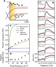
          Modulating light via coherent charge oscillations in solids is the subject of intense research topics in opto-plasmonics. Although a variety of methods are proposed to increase such modulation efficiency, one central challenge is to achieve a high modulation depth (defined by a ratio of extinction with/without light) under small photon-flux injection, which becomes a fundamental trade-off issue both in metals and semiconductors. Here, by fabricating simple micro-ribbon arrays of topological insulator Bi 2Se 3, we report an unprecedentedly large modulation depth of 2,400% at 1.5 THz with very low optical fluence of 45 μJ cm −2. This was possible, first because the extinction spectrum is nearly zero due to the Fano-like plasmon–phonon-destructive interference, thereby contributing an extremely small denominator to the extinction ratio. Second, the numerator of the extinction ratio is markedly increased due to the photoinduced formation of massive two-dimensional electron gas below the topological surface states, which is another contributor to the ultra-high modulation depth.

          Abstract

          For optical control of plasmons metals require a large amount of power in the control pulse, yielding a small modulation depth. Here, Sim et al. fabricate arrays of Bi 2Se 3 and report a modulation depth of 2,400% at 1.5 THz with an optical fluence of 45 μJ/cm 2, demonstrating a novel route for controlling plasmons.

          Related collections

          Most cited references22

          • Record: found
          • Abstract: found
          • Article: found
          Is Open Access

          Topological Insulators in Three Dimensions

          (2007)
          We study three dimensional generalizations of the quantum spin Hall (QSH) effect. Unlike two dimensions, where the QSH effect is distinguished by a single \(Z_2\) topological invariant, in three dimensions there are 4 invariants distinguishing 16 "topological insulator" phases. There are two general classes: weak (WTI) and strong (STI) topological insulators. The WTI states are equivalent to layered 2D QSH states, but are fragile because disorder continuously connects them to band insulators. The STI states are robust and have surface states that realize the 2+1 dimensional parity anomaly without fermion doubling, giving rise to a novel "topological metal" surface phase. We introduce a tight binding model which realizes both the WTI and STI phases, and we discuss the relevance of this model to real three dimensional materials, including bismuth.
            Bookmark
            • Record: found
            • Abstract: found
            • Article: found
            Is Open Access

            Quantum Spin Hall Insulator State in HgTe Quantum Wells

            Recent theory predicted that the Quantum Spin Hall Effect, a fundamentally novel quantum state of matter that exists at zero external magnetic field, may be realized in HgTe/(Hg,Cd)Te quantum wells. We have fabricated such sample structures with low density and high mobility in which we can tune, through an external gate voltage, the carrier conduction from n-type to the p-type, passing through an insulating regime. For thin quantum wells with well width d 6.3 nm), the nominally insulating regime shows a plateau of residual conductance close to 2e^2/h. The residual conductance is independent of the sample width, indicating that it is caused by edge states. Furthermore, the residual conductance is destroyed by a small external magnetic field. The quantum phase transition at the critical thickness, d = 6.3 nm, is also independently determined from the magnetic field induced insulator to metal transition. These observations provide experimental evidence of the quantum spin Hall effect.
              Bookmark
              • Record: found
              • Abstract: found
              • Article: found
              Is Open Access

              Optical nano-imaging of gate-tuneable graphene plasmons

              The ability to manipulate optical fields and the energy flow of light is central to modern information and communication technologies, as well as quantum information processing schemes. However, as photons do not possess charge, controlling them efficiently by electrical means has so far proved elusive. A promising way to achieve electric control of light could be through plasmon polaritons - coupled excitations of photons and charge carriers - in graphene. In this two-dimensional sheet of carbon atoms, it is expected that plasmon polaritons and their associated optical fields can be readily tuned electrically by varying the graphene carrier density. While optical graphene plasmon resonances have recently been investigated spectroscopically, no experiments so far have directly resolved propagating plasmons in real space. Here, we launch and detect propagating optical plasmons in tapered graphene nanostructures using near-field scattering microscopy with infrared excitation light. We provide real-space images of plasmonic field profiles and find that the extracted plasmon wavelength is remarkably short - over 40 times smaller than the wavelength of illumination. We exploit this strong optical field confinement to turn a graphene nanostructure into a tunable resonant plasmonic cavity with extremely small mode volume. The cavity resonance is controlled in-situ by gating the graphene, and in particular, complete switching on and off of the plasmon modes is demonstrated, thus paving the way towards graphene-based optical transistors. This successful alliance between nanoelectronics and nano-optics enables the development of unprecedented active subwavelength-scale optics and a plethora of novel nano-optoelectronic devices and functionalities, such as tunable metamaterials, nanoscale optical processing and strongly enhanced light-matter interactions for quantum devices and (bio)sensors.
                Bookmark

                Author and article information

                Journal
                Nat Commun
                Nat Commun
                Nature Communications
                Nature Pub. Group
                2041-1723
                30 October 2015
                2015
                : 6
                : 8814
                Affiliations
                [1 ]School of Electrical and Electronic Engineering, Yonsei University , Seoul 120-749, Korea
                [2 ]Department of Physics and Astronomy, Rutgers, The State University of New Jersey , Piscataway, New Jersey 08854, USA
                [3 ]Center for Artificial Low Dimensional Electronic Systems, Institute for Basic Science (IBS), Pohang University of Science and Technology (POSTECH) , 77 Cheongam-Ro, Pohang 790-784, Korea
                [4 ]Division of Advanced Materials Science, Pohang University of Science and Technology (POSTECH) , 77 Cheongam-Ro, Pohang 790-784, Korea
                [5 ]Institute for Advanced Materials, Devices and Nanotechnology, Rutgers, The State University of New Jersey , Piscataway, New Jersey 08854, USA
                [6 ]Department of Materials Science and Engineering, Pohang University of Science and Technology (POSTECH) , 77 Cheongam-Ro, Pohang 790-784, Korea
                Author notes
                Article
                ncomms9814
                10.1038/ncomms9814
                4640142
                26514372
                dfac458f-6f4b-4b72-b8fd-88df758c342b
                Copyright © 2015, Nature Publishing Group, a division of Macmillan Publishers Limited. All Rights Reserved.

                This work is licensed under a Creative Commons Attribution 4.0 International License. The images or other third party material in this article are included in the article's Creative Commons license, unless indicated otherwise in the credit line; if the material is not included under the Creative Commons license, users will need to obtain permission from the license holder to reproduce the material. To view a copy of this license, visit http://creativecommons.org/licenses/by/4.0/

                History
                : 29 April 2015
                : 06 October 2015
                Categories
                Article

                Uncategorized
                Uncategorized

                Comments

                Comment on this article